
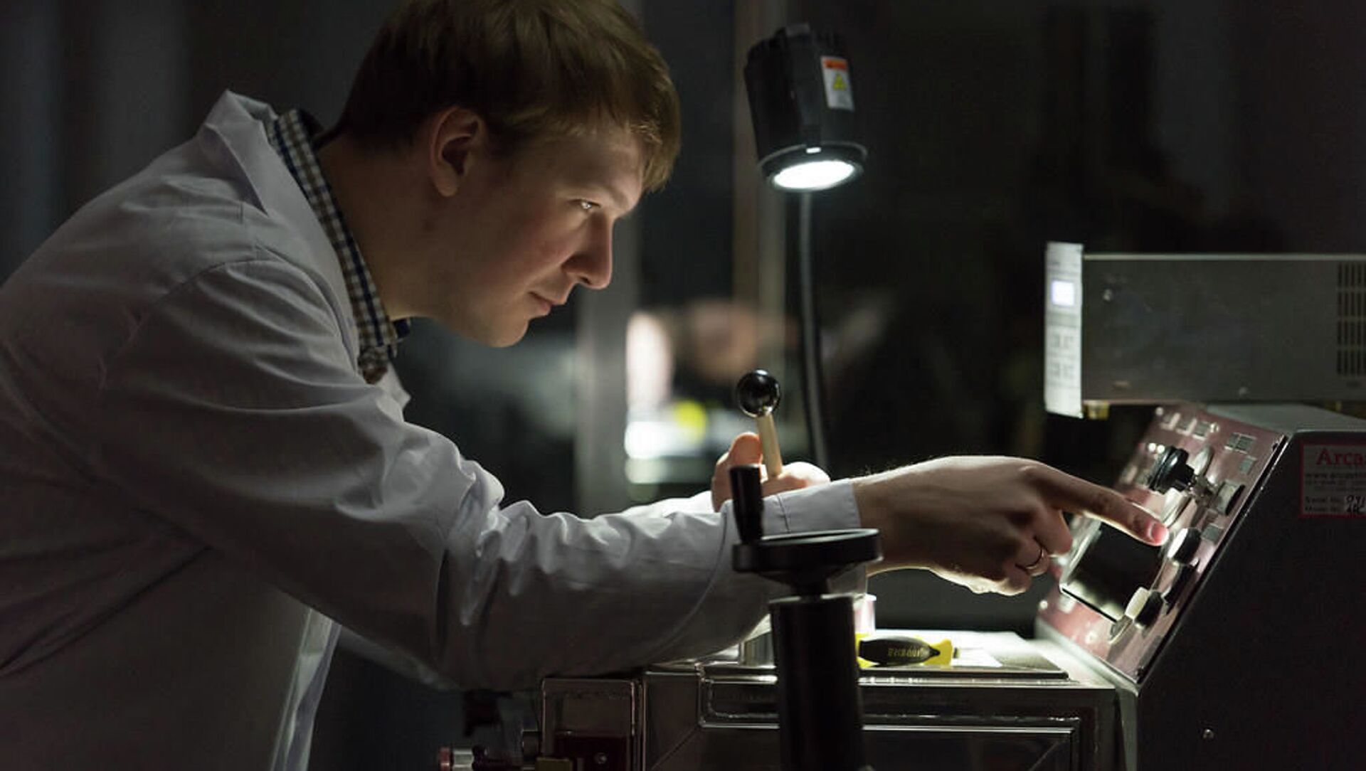
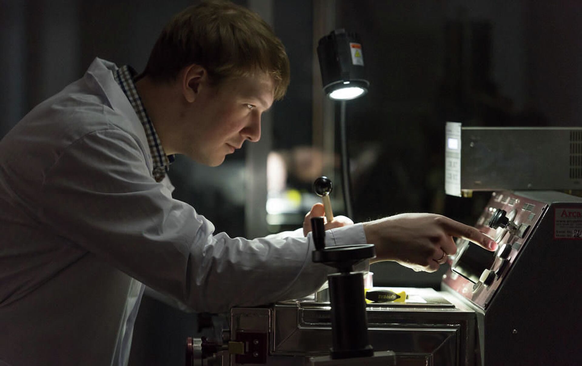
Scientists at the National University of Science and Technology MISiS (NUST MISiS) are actively researching the technology to produce many types of two-dimensional nanomaterials, as well as the material's properties.It's all about the thin layer
Power of the Thin Layer
The main distinction of 2D materials is that all of their atoms are arranged in the surface layer. In terms of chemistry and crystallography, this means they have numerous unsaturated, uncompensated (dangling) bonds. This results in increased chemical reactivity of these materials, making them significantly different from bulk-layered materials in terms of properties. Dangling bonds allow altering the materials' functions via surface engineering.

This problem was solved by introducing new techniques to create "reinforced" (metal-clad) (graphene. Moreover, researchers developed the technology to produce large, defect-free films of graphene that are used as transparent electrodes for various devices. They also developed methods to obtain graphene oxide flakes that are now being implemented as functional fillers for polymer composites.
Graphene's conductivity is most similar to that of metals, making graphene difficult to use in logical circuit elements. That is why scientists are researching other 2D materials, such as transitional metal chalcogenides, for use in electronics and sensors. These materials have semiconducting properties and differ in conductivity type.
Scientists are also researching other complex 2D structures, such as MXenes. They possess a range of properties that are unique for ceramics, as well as high conductivity and plastic deformation properties.
READ MORE: Russian Researchers Invent Highly Efficient Magnetic Refrigerator
In fact, every new 2D material is of interest to science due to its properties, and can be of use in technology.
Deposit, Mill or Flake?
Today, researchers are studying various ways to produce 2D materials. Chemical vapor deposition allows creating high-quality films from many 2D materials (even though this method is rather expensive), while chemical exfoliation of laminated materials can produce several atomic layers of thick dispersions and flakes.
There are methods that involve high-energy milling with planetary mills, as well as complex methods that involve first obtaining intermediate phases and then chemically exfoliating the material to ultrathin flakes. The high-intensity ultrasonic cavitation method can produce 2D structures from bulk-layered materials.
The choice of method significantly affects the resulting material's properties. Thus, chemical vapor or atomic layer deposition methods are most promising for creating electronic devices, as they allow for precise control over the thickness and size of structural elements as well as the purity and morphology of the obtained material.
READ MORE: Russian Engineers Show Possible Replacement for Legendary Makarov Pistol (VIDEO)
Despite the fact that the highest quality films are obtained with the chemical vapor deposition method, scientists Geim and Novoselov initially used sticky tape to measure tiny graphene flakes. Today, ready-to-use dispersions of ultrathin flakes can easily be purchased.
The laboratories are currently working on methods to obtain other materials. As soon as the scientists find the most promising area for implementation, the relevant technology will follow.
2D Materials in Russia
Researchers at the NUST MISiS' Functional Systems & High-Temperature Materials Department are currently developing transition metal chalcogenides for solar cells, LEDs and sensors, and studying graphene oxide as a coating designed to improve corrosion resistance in various types of steel. They are also researching ways to obtain the layered structures of titanium and vanadium carbides called MXenes; they have achieved some interesting results.
"Our group's cooperation with Professor Aldo Di Carlo at the University of Rome Tor Vergata in 2D nanomaterial research resulted in a mega grant and establishing a new laboratory," said the department's senior research fellow Dmitry Muratov to a RIA Novosti representative. "A large portion of the research carried out in the laboratory is aimed at using several types of 2D nanomaterials to create perovskite solar cells."
Muratov believes this to be an example of efficient cooperation: as material scientists synthesize and research the best new materials and their properties for use in solar cells, the researchers specializing in semiconductor devices are creating these cells and exploring their operational parameters.
"Moreover, we are cooperating with Andrei Stepashkin's group, at the NUST MISiS Center of Composite Materials, to obtain and research the composites' properties," Muratov added. "I have presented reports on our work on composites with nanostructured boron nitride to our foreign colleagues before; for example, in Spain, at the International Symposium on Metastable, Amorphous and Nanostructured Materials (ISMANAM)."

To do this, they used high density polyethylene filled with hexagonal boron nitride, modified to achieve the necessary properties. In terms of recycling, the obtained materials turned out to be better than their more popular counterparts; plus, they can mitigate the tendency of printed circuit boards to overheat.
International Cooperation
Today, NUST MISiS is promoting cooperation with the University of Nebraska-Lincoln (USA) in creating 2D materials and studying their properties. This cooperation was launched upon the announcement of infrastructure development contests organized within the framework of the 5-100 Project federal program. These contests involve using leading scientists to manage the research teams and carry out research in promising areas.
"We invited Professor Alexander Sinitsky, who is currently working full-time at the University of Nebraska-Lincoln," Muratov explained. "In 2016, we submitted a proposal to one of the contests together to work on 2D materials, and we won it. We began cooperating after this; within its framework, I underwent training at Alexander's laboratory in the US in order to use the obtained knowledge to create an experimental database here in our department."

The scientists published the results of their research on molybdenum dioxide (MoO2) in the scientific journal Nanotechnology.
Using chemical vapor deposition synthesis, they obtained the 2D material and thoroughly researched it with analytical methods. Another example is the article on titanium sulfide published in the ACS Nano Journal.
"We have achieved very good results on the material's conductivity as well as the possibility of obtaining very thin, conductive layers of MoO2 (crystals, in this case) that are stable in the air, on substrates that are different by their nature," Muratov stated. "We will use these findings in further studies."
The new material can be used to create various heterostructures and nanodevices — transistors, sensors, photodetectors and more. Today, the materials created at NUST MISiS in collaboration with the University of Nebraska-Lincoln are being implemented as transport layers in thin-film solar cells, LEDs and sensors. The scientists are also working on creating polymer matrix composites filled with 2D nanomaterials.


