
The new research, which was published in the Nature Physics journal, became the latest advance toward creating electronic devices with controlled properties.
Today, the study of two-dimensional materials (two-dimensional systems are systems where the movement of electrons in confined to the xy plane) is one of the main priorities of scientific research. That is why the scientists who discovered and researched the first such material (graphene) were awarded the 2010 Nobel Prize in Physics.
READ MORE: Russian Scientists Working on Online Speech Rehabilitation System
Due to these properties, scientists use two-dimensional materials as a basis for elements used in next generation compact electronic devices. For example, two-dimensional molybdenum disulfide (MoS2) has high charge mobility plus high on/off ratio in field-effect transistors, which means that this material can be used to significantly increase the operating speed of electronic devices.
In 2017, full application of this material came very close to the mechanism for repairing defects in MoS2 monolayers described by Professor Gotthard Seifert in his research published in the ACS Nano journal. Scientists have continued studying properties of two-dimension materials.
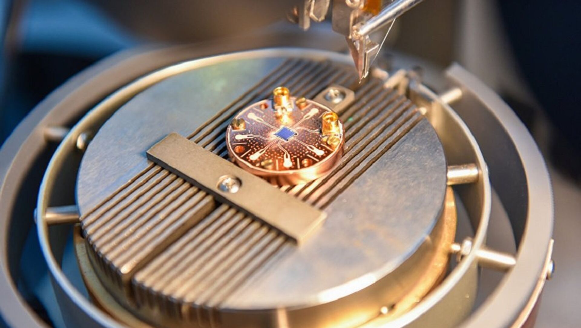
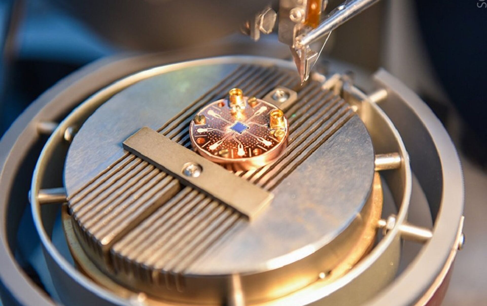
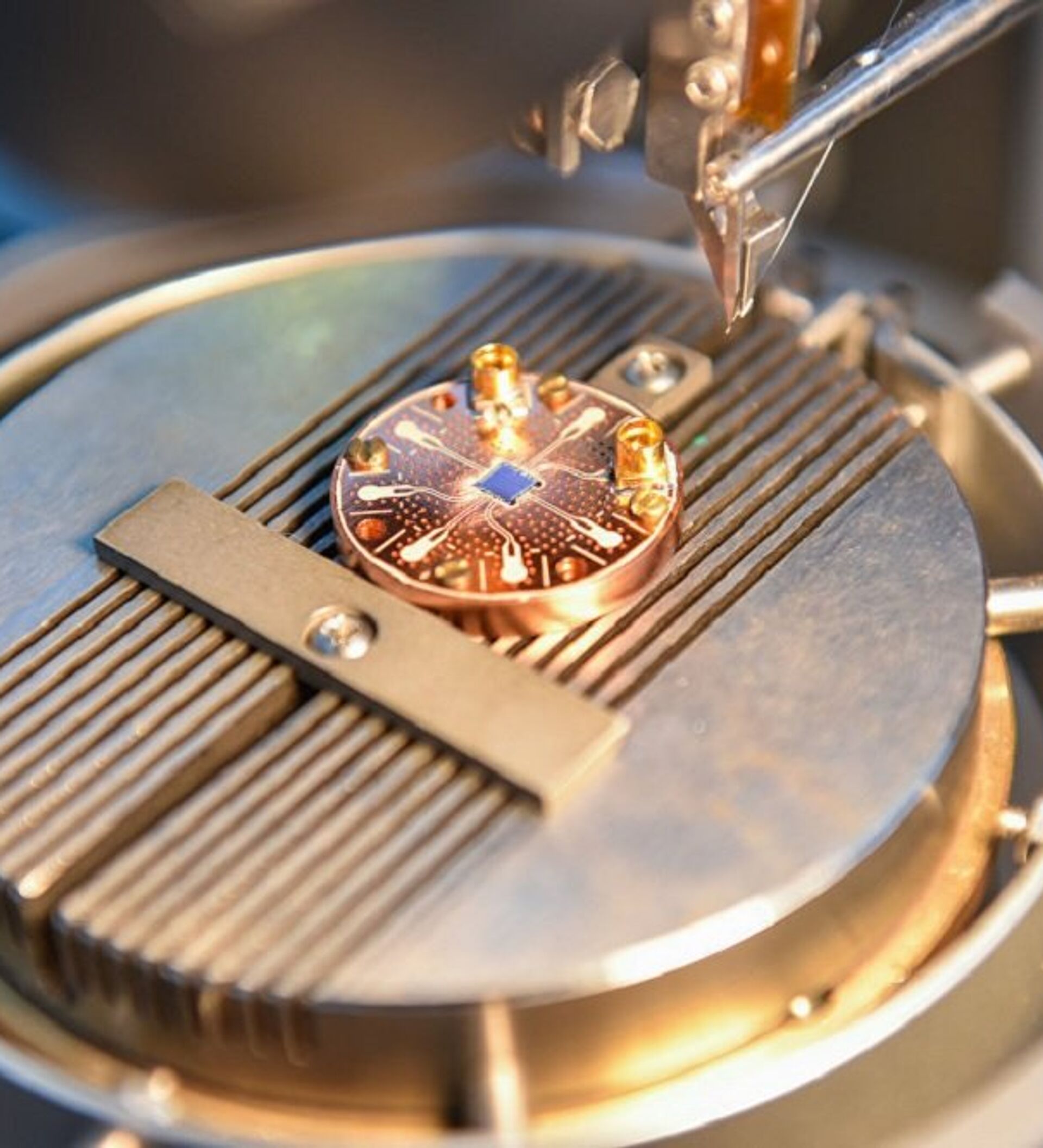
"The exceptional optical properties of molybdenum disulfide (MoS2) and tungsten diselenide (WSe2) monolayers are caused by tightly bound electron-hole (quasiparticles carrying positive charge) pairs called excitons," explained NUST MISiS Professor Gotthard Seifert.
Creating MoS2/WSe2 heterostructures by stacking individual monolayers results in the emergence of a new type of excitons, where the electrons and holes are spatially separated into different layers.
"With the help of spectroscopy and quantum-chemical calculations, we identified a partially charge-separated electron-hole pair in MoS2/WSe2 heterostructures, as well as its location," said Seifert. "We managed to control the emission energy of this new type of exciton by varying the relative orientation of the layers."

Seifert states that the team of researchers is planning to continue studying how the rotation of layers affects the materials' electronic properties and what exactly can be created with the help of these materials: solar panel elements, transistors or various other devices.


