

Experts from the National University of Science and Technology MISIS (NUST MISIS) working under the supervision of Pavel Sorokin, DSc (Physics and Mathematics), implemented the theoretical aspects of this research project. Their US colleagues working at Tulane University, New Orleans, Louisiana, under the supervision of Professor Jiang Wei, completed the experimental part.
Pavel Sorokin, Head of the Theoretical Materials Science of Nano-Structures Infrastructure at the Inorganic Nano-Materials Laboratory at NUST MISIS, DSc (Physics and Mathematics), is interviewed by a RIA Novosti correspondent and discusses the future influence of this "smart material" on human life.
Mr. Sorokin, the theoretical aspect of this research project, completed under your supervision, is linked with another technological leap. What is its essence? How will semiconductors of the future differ from their current versions?
Pavel Sorokin: Indeed, our two research teams working on opposite sides of the Atlantic Ocean have managed to take a joint step toward more compact and more rapid electronics. Theoretically speaking, it will become possible to reduce electronic circuits down to nano-sizes using this new material; at the same time, devices utilizing these circuits will operate more quickly.
These systems will consume less power, and their structure and design will also change. But, first of all, the range of their functions will expand.
You see, any device's speed and other parameters are directly proportional to the quality of current-conducting materials in the device. We have managed to disengage compact nano-wires from the new connection, and this gives us reason to hope that it will be possible to use them in new electronic nano-devices, whose very creation will be linked with the future of this entire technology.

What sectors of the electronics industry will change drastically with the advent of the new nano-sized "construction material?"
Pavel Sorokin: This material will be mostly used in opto-electronics and microelectronics. Smaller materials often make it possible to achieve extraordinary electronic, optical, mechanical, chemical and biological properties using quantum confinement and surface effects.
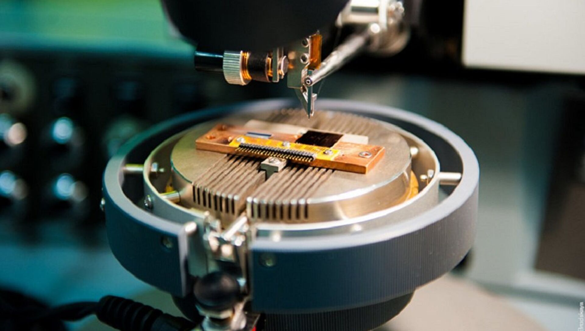
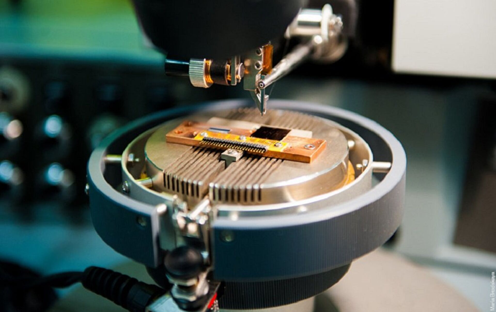
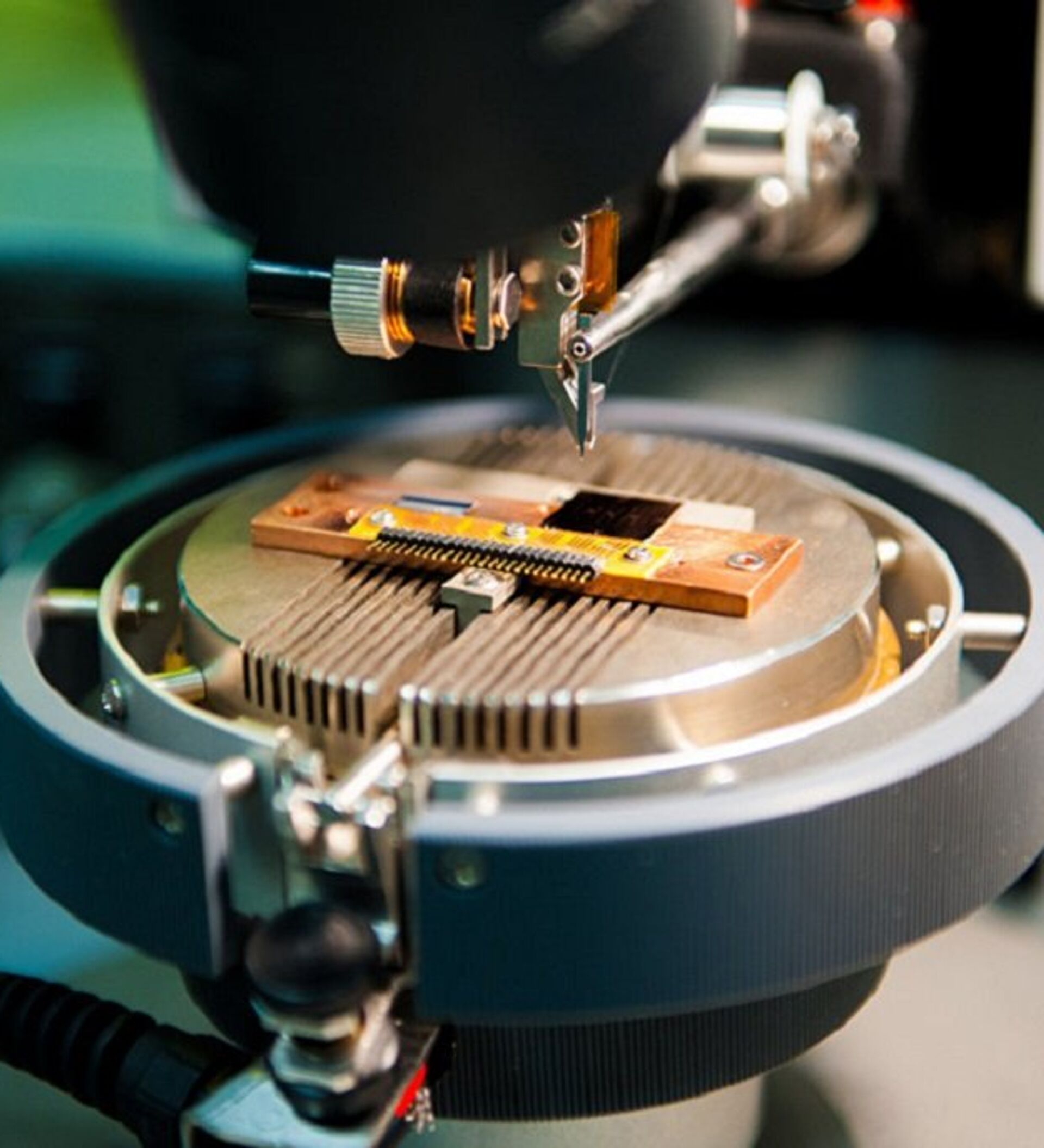
Our work has impressive practical significance because this one-dimensional nano-structure that we have obtained can boast of a very small diameter. At the same time, objects with this diameter are obtained using a method that we can carefully control. Our approach differs completely from previous methods, which were focused on cutting graphene and di-chalcogens into separate ribbons. And this is the considerable advantage of the materials that we've discovered.
The crystal consists of interlinked nano-structures and nano-ribbons; at the same time, all nano-ribbons have a uniform width. Therefore we will always obtain ribbons with one and the same width, while streamlining the crystal-stripping process. It is becoming possible to continually produce these results.
I cannot help asking: What compels a scientist to make a discovery? Does a discovery suddenly come to him, or does this happen as a result of his thinking long and hard about something followed by research by trial and error?
Pavel Sorokin: It all began in 2010 during my post-doctoral studies at Rice University in Texas. I worked with a team headed by the outstanding expert Professor Boris Jacobson who relocated to the United States from Russia long ago. He always taught us to look at things from different angles, to seek out new aspects in areas that are supposedly already well-studied.
I believe that I received an excellent education under his guidance, lifting me to a level above the already exceptional training I received in Russia while studying with the brilliant scientist, Leonid Chernozatonsky. While at Rice University I got acquainted with Jiang Wei, a young but extremely talented and active post-doc. Three years later when I was back in Moscow I received a letter from him proposing that we work together. Our cooperation began with a joint article published in the Nature Physics journal.

Although discovered in the 1980s, this complicated tantalum-palladium (platinum)-selenium compound (Ta-Pd-(Pt)-Se) was nevertheless not studied in great detail. The crystal consists of weakly linked ribbons, whose structure is similar to di-chalcogenide ribbons of transition metals.
Scientists have been interested in the two-dimensional compound of di-chalcogenide of transition metals for a long time, and with good reason because di-chalcogenides of transition metals, including molybdenum disulfide or tungsten disulfide, boast semiconducting properties. This makes it possible to consider them as materials capable of becoming the basic element of semiconducting electronics in the post-silicon era.
This compound's structure resembles a "sandwich" with three atomic layers: chalcogen, such as selenium or sulfur, followed by a layer of transition metals' atoms, such as tungsten or molybdenum, and by chalcogen once again.
So we have obtained a two-dimensional layer of the di-chalcogenide of transition metals with semiconducting properties. But we think there is still progress to be made and we continue trying to make it one-dimensional. Our goal is to reduce its thickness and width and to create the smallest possible semiconducting element using the two-dimensional layer as our foundation.
And that's when we started facing problems. It proved impossible to effectively cut up the layer into thin nano-wires and to obtain a one-dimensional structure from a three-atom layer substance. That "sandwich" crumbled apart time and again, and the parameters of cut-up ribbons did not suit us.
Somewhere in 2004, the academic community first focused on graphene as the main candidate for a 21st century semiconductor. How did you come to the idea that perhaps you should start looking at other materials?
Pavel Sorokin: We simply realized that the formula of this "stubborn" substance was quite similar to the structure of di-chalcogenides of transition metals and it dawned on us that this is exactly the nano-ribbon we were looking for. And now all that remains is to break up the initial crystal into its components.
My colleague Jiang Wei accomplished this. To put it in simple terms, he basically pasted a piece of scotch tape to the crystal, pulled it away and obtained the required nano-structure. This method was at one time also used to obtain graphene. Despite its simplicity, it is quite effective and makes it possible to obtain high-quality nano-structures.
That was how Jiang Wei made the first wires measuring about one nanometer thick. He virtually reached the level of that ribbon. After that, our US colleagues made the first transistor from that material. At the same time, people in Moscow studied the electronic and structural properties of separate ribbons and nano-wires (several interlinked ribbons).
Our work is far from over. So far, we have obtained several interlinked nano-ribbons. In any event, we hope that our research project will pave the way toward discovering new nano-structures because the tantalum-palladium-selenium compound is just one member of a big family of these promising materials.


