

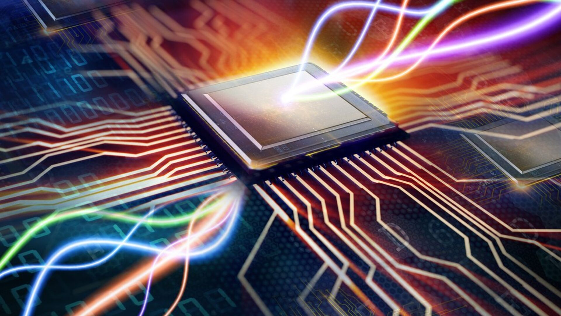
Indian scientists have developed a computational tool to evaluate the performance of advanced graphene-like two dimensional (2D) materials. It helps pre-evaluate the performance of advanced materials and checks their suitability for a device before manufacturing them.
This helps understand a material’s electro-physical properties before the device is fabricated, saving time and money, and there is a high demand for such tools.
The sophisticated tool can predict along which directions some 2D materials could display minimal scattering, thereby improving the performance of nanoscale devices, said the scientists involved in the development of the tool.
“In the semiconducting channel of a device such as a transistor, electrons (hole) carriers transport the charge (and information encoded within the charge) from the input to the output end. The phonons interact with carriers during this transport and create ‘resistance’, which affects the performance aspects such as drive current and the speed of operation. The strength of such interaction is material-specific, and thus it is crucial to understand when we plan to design transistors fabricated with 2D materials,” explained Dr Santanu Mahapatra, team lead of the study, and professor at the Bengaluru-based Indian Institute of Science, while speaking to India Science Wire. The results of the study were published in the Journal of Applied Physics.
The study offers one such model to evaluate the electron-phonon interactions in the material. In a semiconductor, at the quantum level, two systems exist, the electron-hole charge carriers and another system called phonon, that originates from the lattice vibrations.
Electron-phonon coupling limited transport is a complex process, and in this study, the low-energy two-band model was used for computations.
The team employed a software tool called VASP to analyse the energy band structure of different materials. They developed the extensive software code by using Hybrid C and MATLAB programming styles.
The scientists demonstrated the performance of a phosphorene based MOSFET (building blocks of ICs) using the simulated model. The atomic structure of the material has a web-like distribution where the atoms are patterned in a sequential form (called the armchair format) and also in a zig-zag fashion. They observed that for phosphorene, electron-phonon scattering is more pronounced in the zig-zag direction.


